(mostly) 4th Gen x86 Shootout!

Having recently restored my old 486SLC board, I was curious how it stacked up against other 486s of the era. I actually have a fairly decent collection of chips from this time period and a few motherboards that accept them.

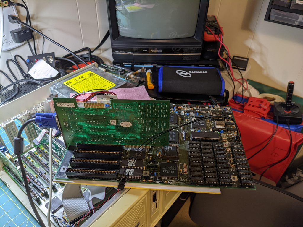
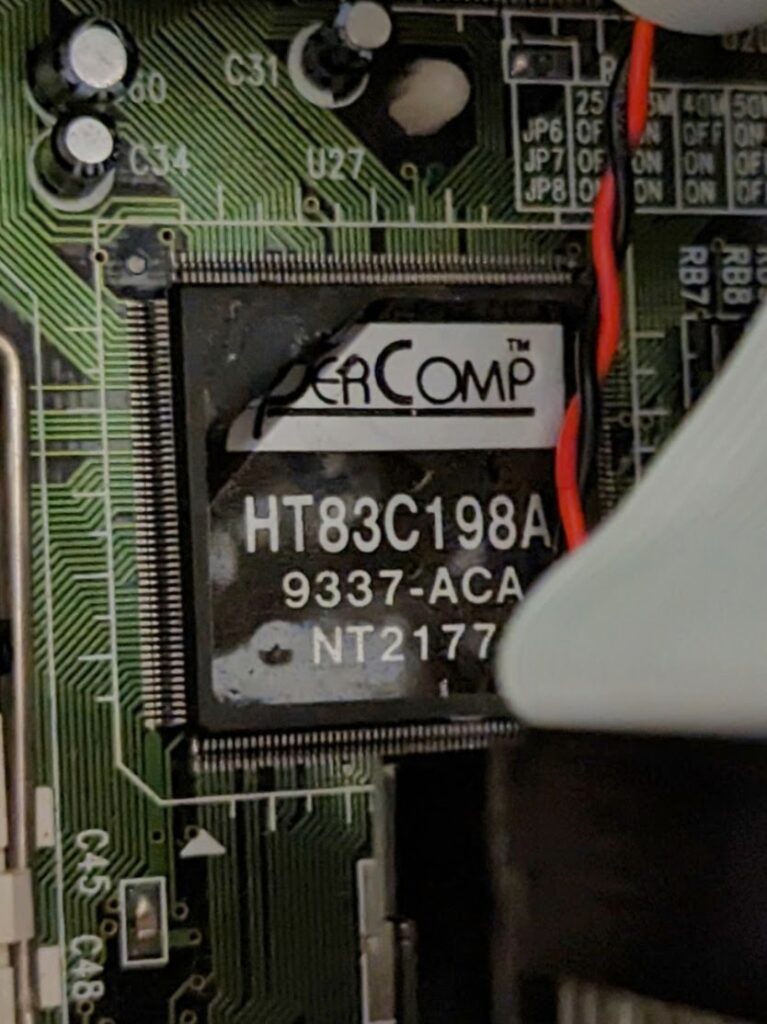
For the majority of this test, I used a PerComp branded board made by PC Chips, (model M912) that has a fairly broad range of support for these CPUs and is based on the PC Chips “Chip 16″/”Chip 18” chipset. The board is configured with 256KB of L2 cache, 16MB of 32-pin SIMM memory and supports 7x 16-bit ISA expansion slots, 3 of which support 32-bit VLB cards.

stock photo of an unlabeled M912 board

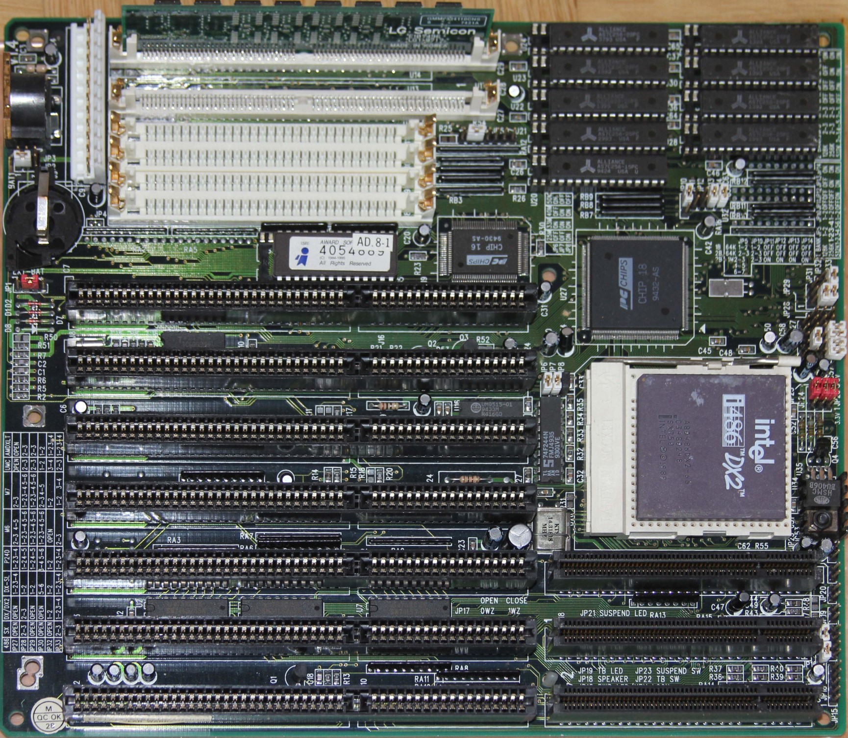
One funny thing about this board is the branding on the chipset. At the time PC Chips didn’t have a great reputation for performance. In an attempt to boost their sales, they often placed stickers on their chips with the model numbers of other more popular chipsets.

fake chipset branding
actual chipset branding

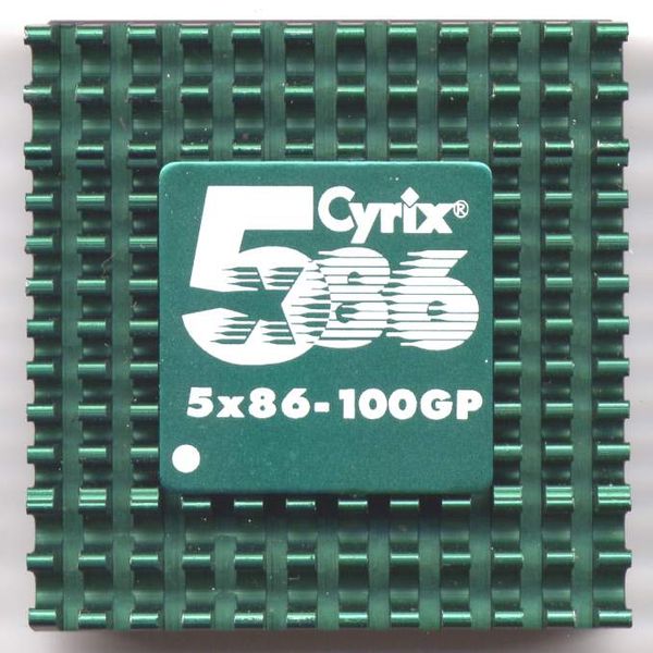
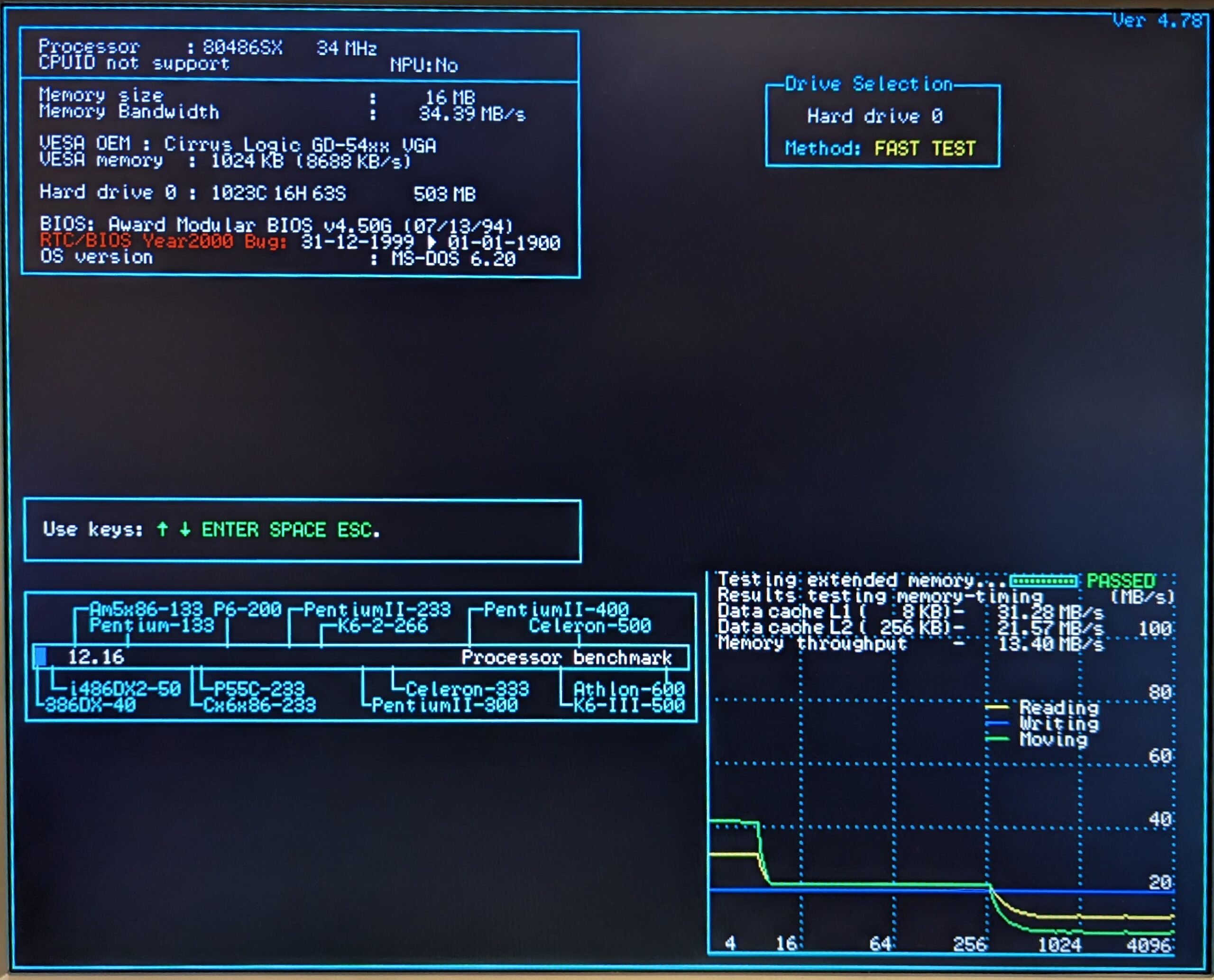
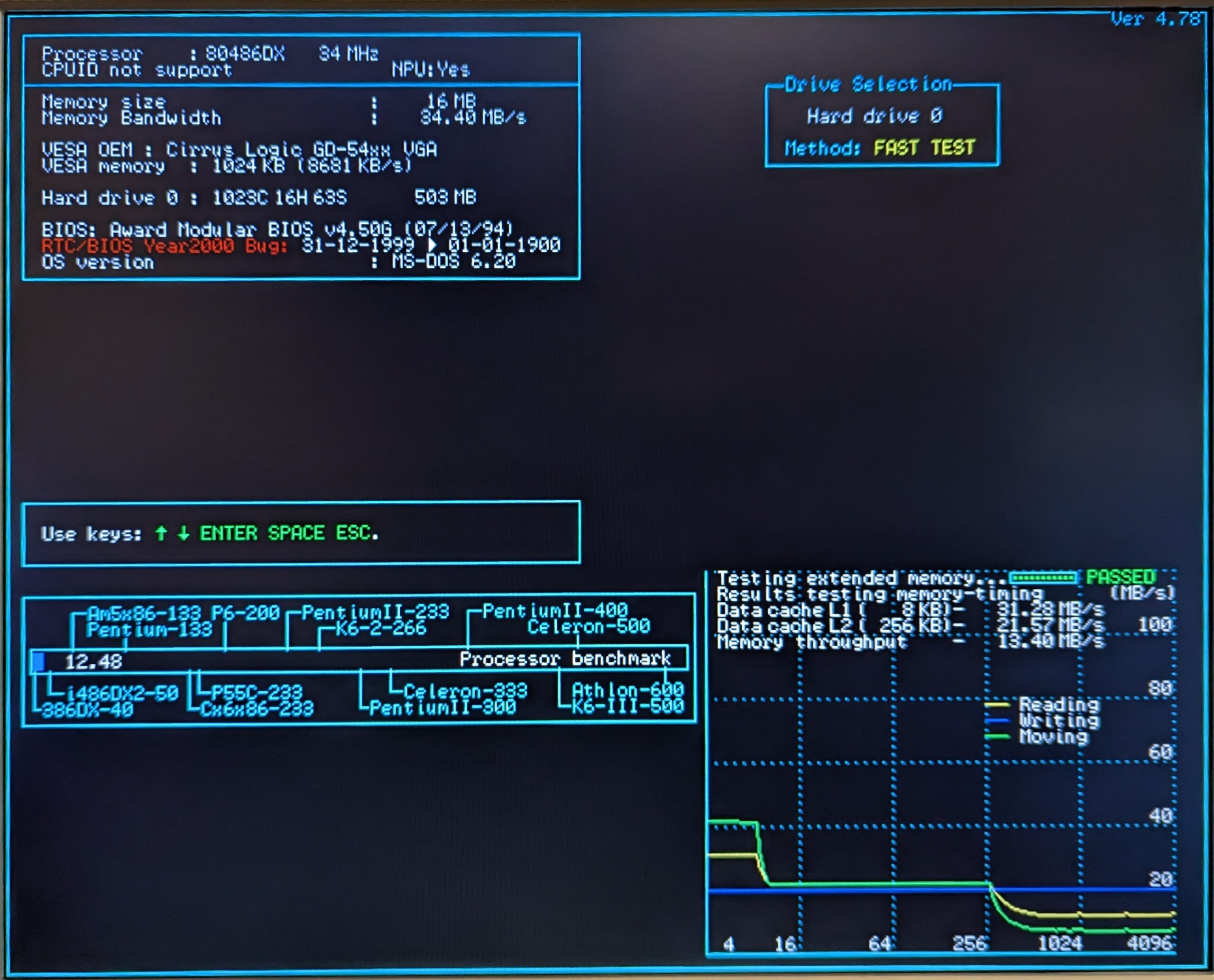
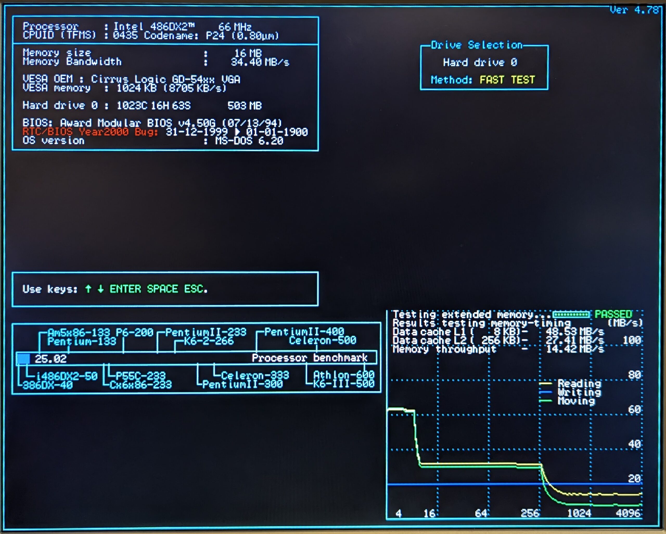
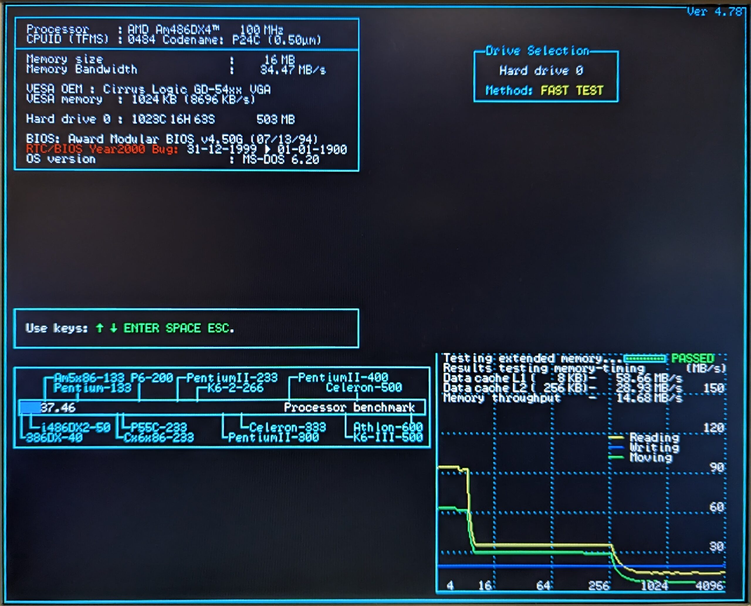
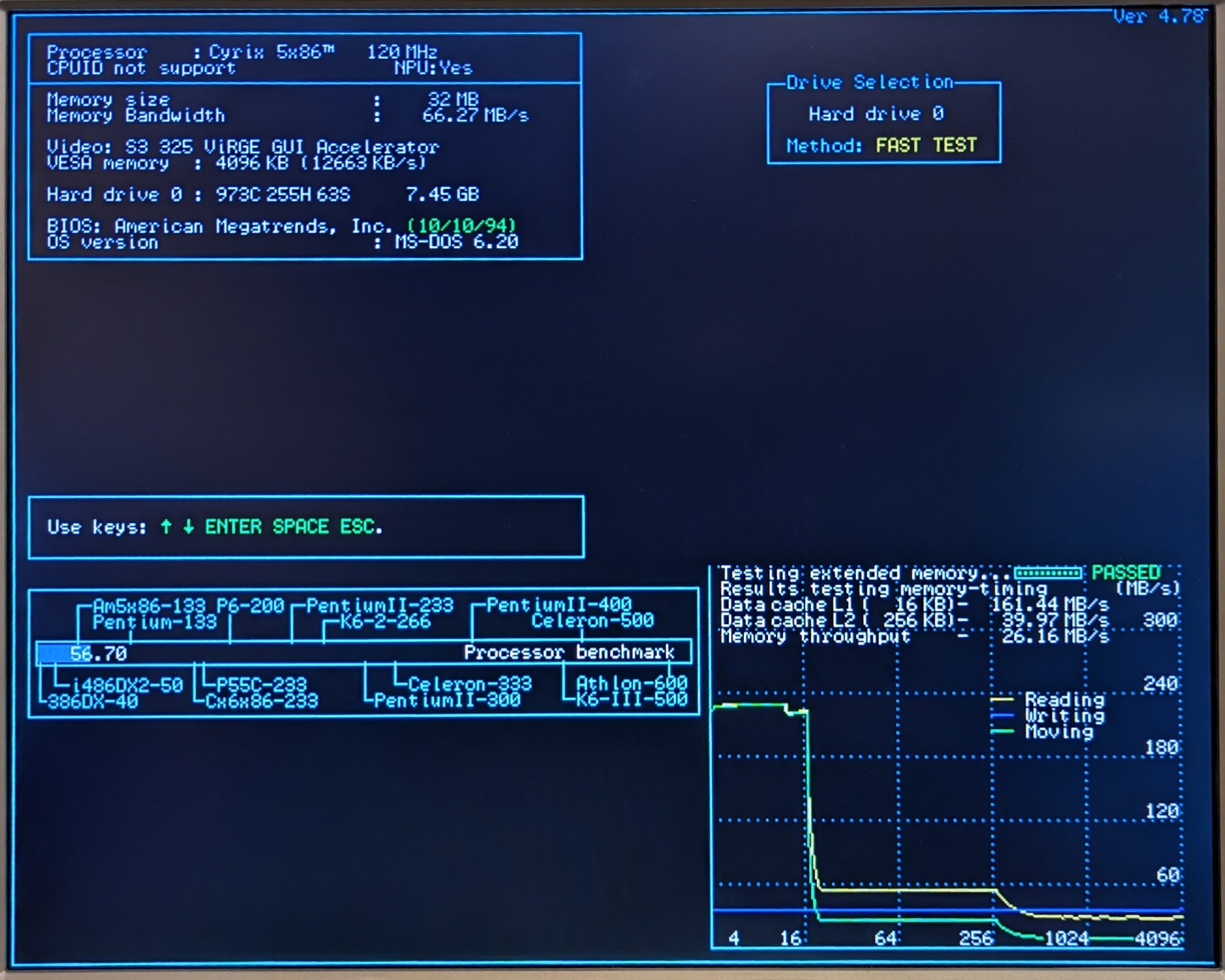
Alright, enough of the history… let’s get into the testing! The chips I selected for the test were several Intel CPUs, a couple of Cyrix CPUs and a single AMD CPU. These were as follows: i486SX-25 (overclocked to 33Mhz), i486DX-33, i486DX2-66, Cx486DX2-66, Am486DX4-100, Cx5x86-100 (overclocked to 120Mhz)

stock photo of the chip I have. Mine has a fan bolted onto the heatsink as I’ve overclocked it to 120Mhz

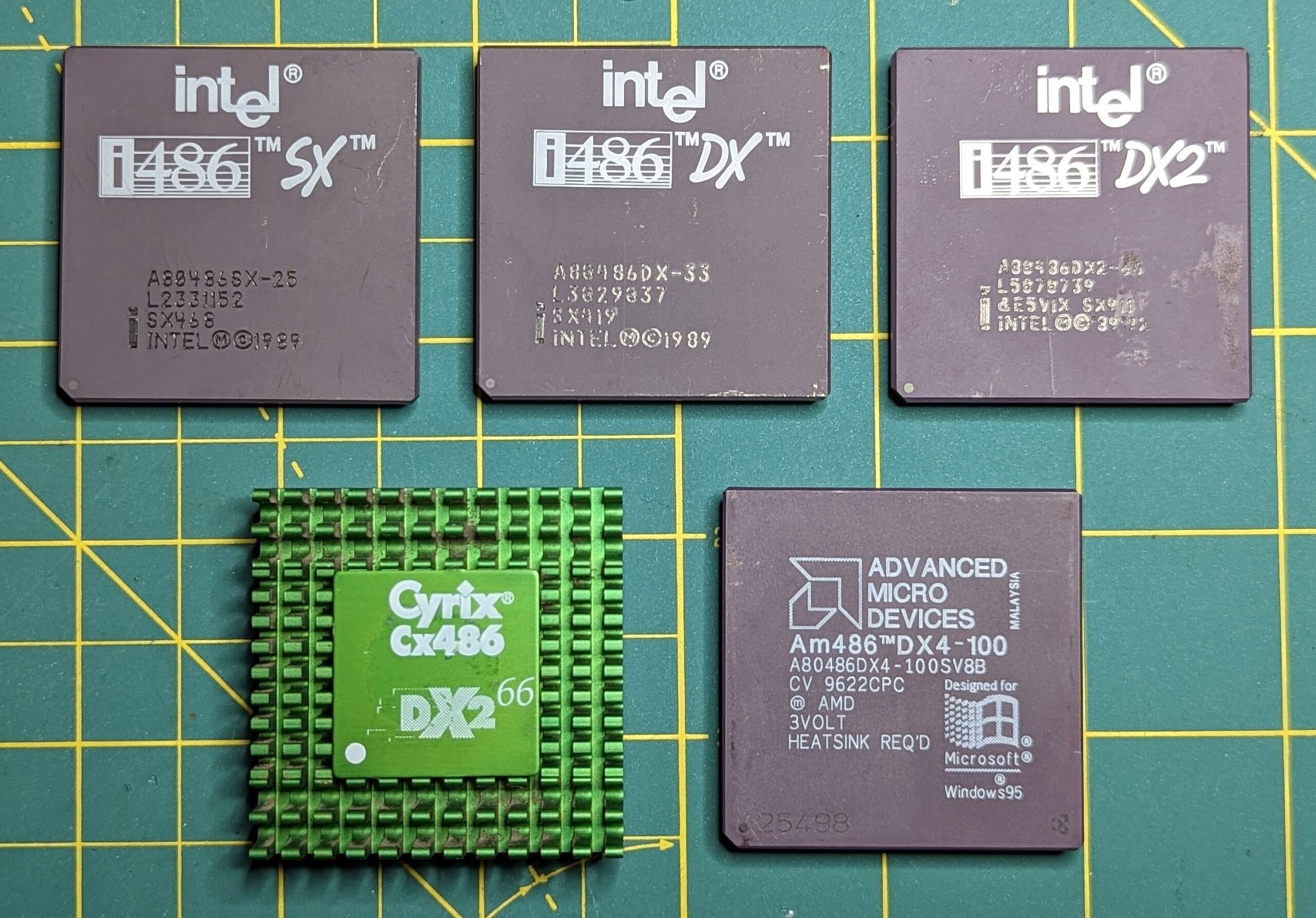
The five 486 CPUs shown above all contain 8k of L1 cache on-die. They were all tested on the same motherboard mentioned above, which was configured with 256k of L2 cache.

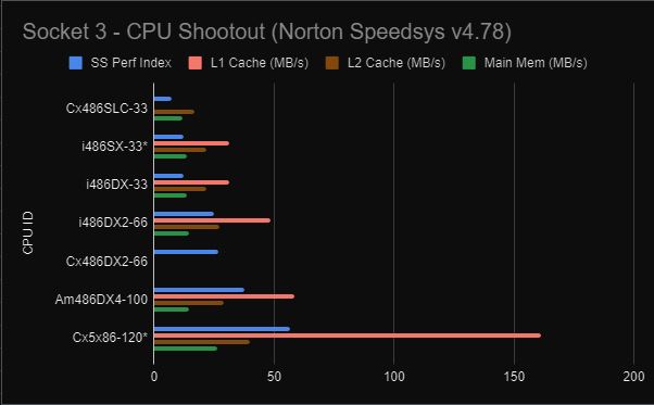
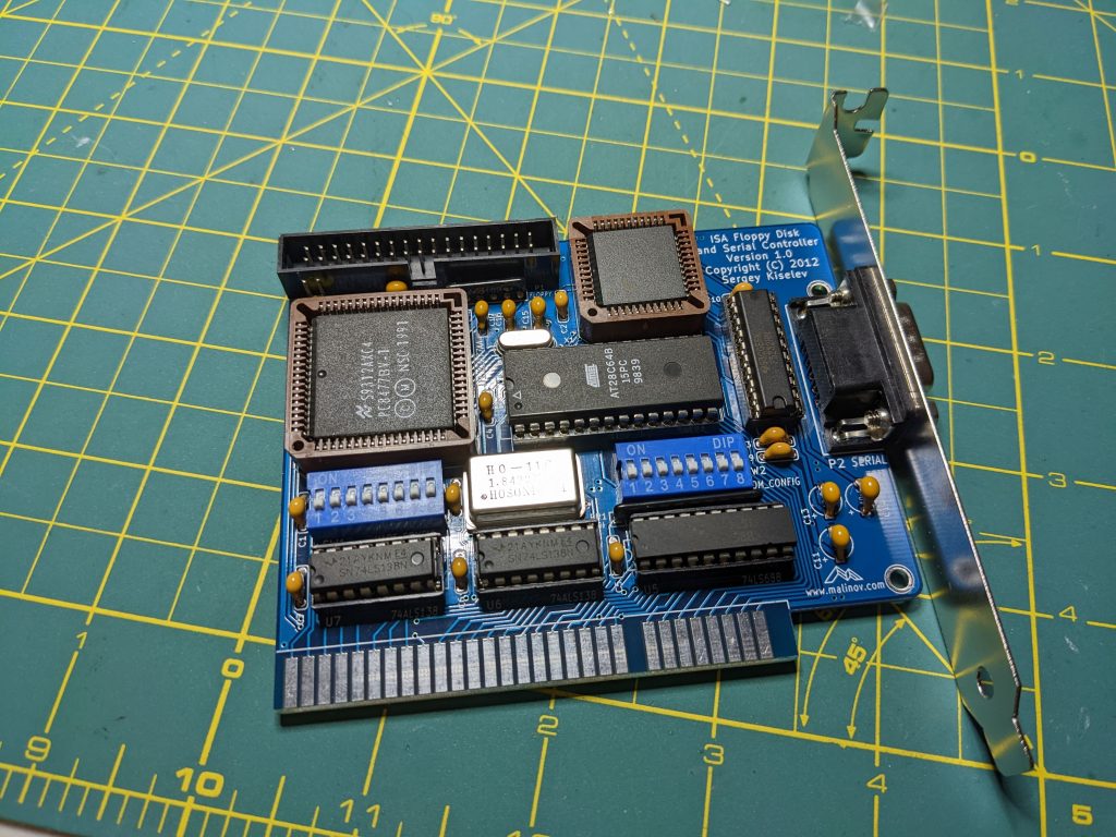
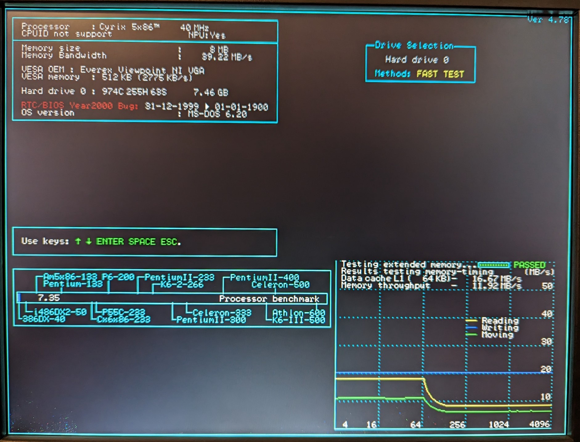
I’ve also included the 486SLC numbers from a previous test. The SLC and the 5×86 aren’t a good direct comparison since the motherboard and configurations are quite different. Unfortunately, I managed to kill the Cyrix 486DX2-66 when I tested it the second time and wasn’t able to get cache and system performance numbers, but an image with the last screen it produced is included below.

What was most interesting to me were the results for the Intel SX and DX chips clocked at 33Mhz. All of the results from these 2 chips were identical except for the performance index. (which is lower on the SX as it lacks an FPU) What this tells me is that unlike the 3rd generation, Intel’s 4th generation SX chips were fully 32-bit externally. The i386SX was 16-bit externally and was dramatically slower as a result. Likewise the Cyrix 486SLC also suffered in this test due to its 16-bit external bus. I suspect Intel’s 4th generation SX chips were simply lower binned parts from the DX production line that had defects in the FPU section of the die. Simply disabling the FPU by cutting/burning the traces between it and the CPU section of the die would allow these otherwise defective chips to be sold, albeit as a lower-end model.

TX486SLC-e w/IIT FPU
i486SX25 @33Mhz
i486DX-33
i486DX2-66
Cx486DX2-66
Am486DX4-100
Cx5x86-100 @120Mhz

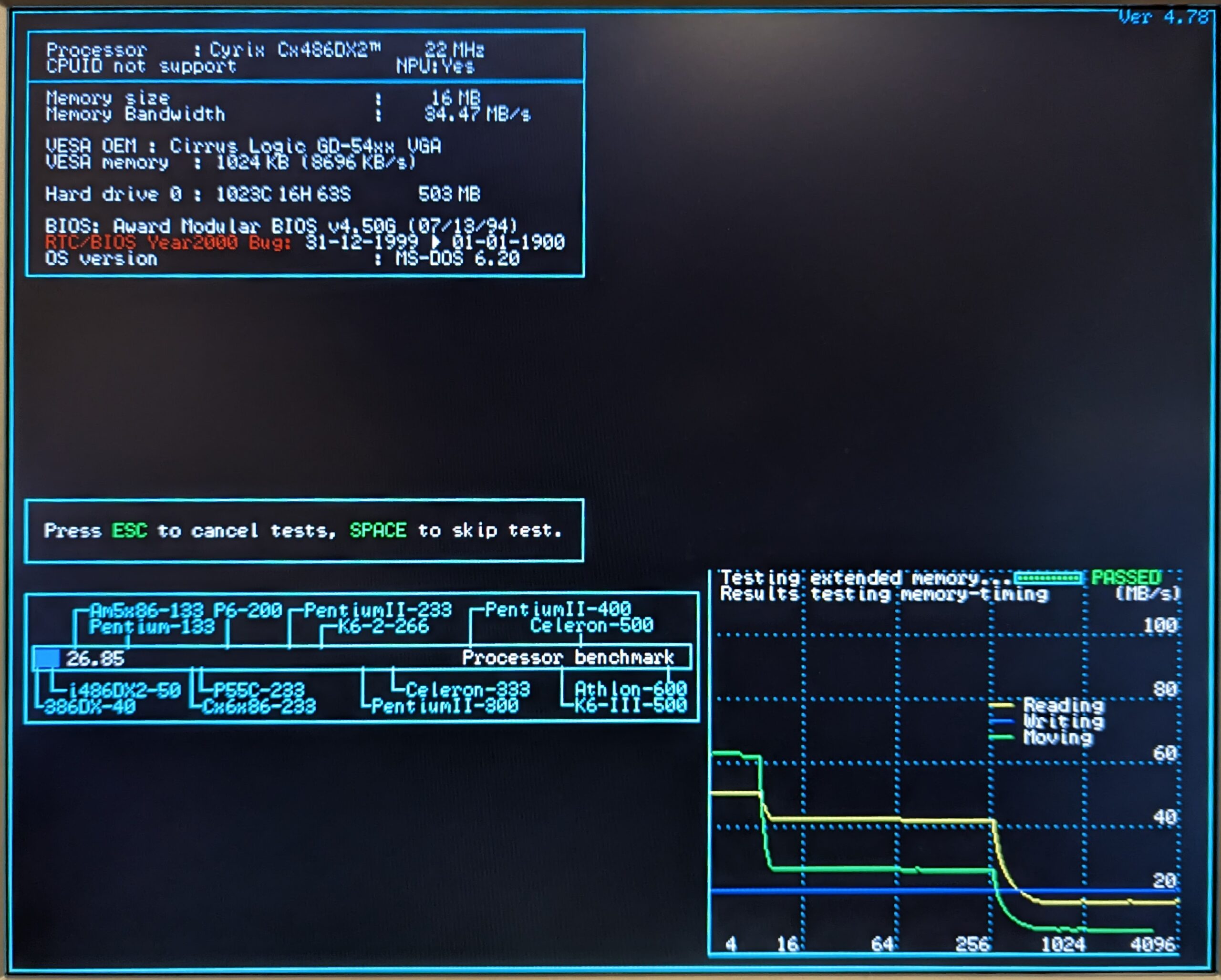
It’s a shame the Cyrix DX2-66 gave up the ghost during the test. However, it’s not a chip I was likely to put back into use in any of these systems. What data I did get from it confirmed my recollection of the CPU. It was slightly faster than the Intel DX2-66 in integer ops, but was a bit slower in floating point due to a weaker FPU design.

Building custom boards for retro PCs

In my last post I went through the process of bringing an old 286/12 back to life. At the end of that post, I left off with the machine unable to boot from it’s own hard disk. This meant I would need to find another way to allow an old machine like this to boot from more modern media. Thankfully I found a solution in an open source hardware kit called the XT-IDE. The XT-IDE kit is a very simple 8-bit ISA hard disk controller for IDE drives that coupled with some firmware allows XT/AT & clone computers to boot from larger drives. Since this board is only a hard disk controller, I would also need a floppy controller. (more on that later) I ordered up a kit and when it arrived, I immediately tore into the package and built it up.

This being the 4th revision of the board, it was an incredibly well polished design. I did actually have to add some pin headers for the jumpers which were not included with the kit, so just keep that in mind if you build one of these. I read over the instructions for assembly just to be sure, but the board has such a nice silkscreen it almost isn’t necessary. Assembly went relatively quickly with the board completed in about 1.5hrs.

With the board assembly complete, I put it under a crafting lamp with a magnifying glass and inspected all of the solder joints to look for any bridges and touched up anything that didn’t look quite good enough. After that, it was time for the moment of truth. I plugged it into the 286, connected up the hard disk and it actually booted into DOS from the hard drive! For this test, I had actually kept the multi-i/o board installed, but with the IDE section disabled. (just in case I needed the floppy)

Speaking of floppy disks… I didn’t want to keep the multi-i/o controller in the 286 as I planned to return it to the 486SLC where it belongs. (and it’s my only surviving multi-i/o board of this type) Having had so much success with the XT-IDE and given the prices of original floppy controllers from this era, I decided to see if there was another open source controller option for floppy disks. Sure enough, I found that someone named Sergey Kiselev had designed just such a board. I ordered a complete kit from eBay and built it up with the same enthusiasm as the XT-IDE.

This kit was based primarily on a pair of PLCC chips and was a more compact design than the XT-IDE. This made assembly a bit more difficult as there were more connections closer together. I initially tacked the parts in place by soldering just 2 connections each and then went back later to fill in all of the rest. The sockets that came with this kit were the cheaper single-wipe type. I don’t mind these for the smaller DIP chips, but I replaced the one for the ROM with a nicer round hole socket that I had on hand. I also made a small mistake you can see above in that I forgot to socket the larger crystal oscillator, so it’s permanently on the board.

Overall, I’m pretty happy with how the Floppy/Serial controller turned out. I did end up having to change the configuration to make this card play nice with the XT-IDE, but thankfully this is well documented online. All of the chips fit in their sockets really well and the board aligns decently with the ISA slots on the motherboard.

I added a Teac 1.2mb floppy drive (also from eBay) to this system for additional authenticity. (and also because my existing Matsushita drive is finicky when it comes to reading 360k floppies) The open source controller works great so far and it performs just as you’d expect any other floppy controller to function. I’m not currently using the built-in serial features as the DTK 286/12 motherboard actually includes onboard serial and parallel ports. It was really nice to be able to read some of my older floppies that were previously unreadable. At some point I’ll have to see if I can source some DS/HD floppy disks to format at 1.2mb as I never really tried them as a kid. I pretty much jumped straight from 360k floppies to 1.44m 3.5in disks.

These were both fun little projects that made my DTK 286 restoration project complete. If you’re in the process of bringing an old XT or AT machine back from the dead and have similar needs, I highly recommend these kits as they’re inexpensive, fun to make and work really well.

DTK 286/12 board repair and restoration

I’ve been on a bit of a retro restoration kick lately and decided to take a look at a couple of motherboards I’d saved from my childhood. The boards were from my first 2 PCs, an XT clone and an AT clone. At some point towards the end of college, I was running out of space to keep the older computers I had collected to that point. Rather than give up my first machines entirely, I decided to strip them down and save the core parts and interesting bits that still worked and trash the rest. (something I now regret as these parts have become quite rare and expensive)

Fast forward a few decades… these parts have been sitting, stored in the attic and the room over my garage. Interested to see if they still worked, I pulled the motherboards out of their anti-static bags only to discover a horror common to many retro computer enthusiasts. A CMOS battery had leaked and corroded a small, but important section of the board. Back in the old days of IBM-compatible PCs, manufacturers used to include a rechargeable 3.6v battery, (typically Ni-Cd) soldered to the board. These were great and often lasted well beyond the design life of the system, however they became a liability later in storage.

Sadly, I didn’t think to take pictures of the damage when I discovered it, but moved to quickly get rid of the old leaky battery and proceeded to clean up the board with isopropyl alcohol. The acid crystals and much of the corrosion came off of the board, but what became obvious was that a lot of damage had been done. During the time that acid was sitting on these components, it was eating through the metal contacts and traces of the board and its components. This included several sets of jumper pins, a large 40-pin socketed DIP chip, a 1″ PLCC socketed chip and other associated logic chips.

The 40-pin DIP socket was closest to the battery and took the most damage with several of it’s pins and sockets completely disintegrating when I tried to clean them up. Most of the jumper pins cleaned up with a fiberglass brush and I was able to leave them in the board. (though I did have to replace all of the jumpers as they were too far gone) The next big worry was the PLCC chip and its socket as well as a few of the logic chips under it. One of the logic chips was pretty badly corroded, but stayed intact when I cleaned it. I cleaned up the contacts as much as possible with the fiberglass pen and attempted to flow some new leaded solder into the vias in the hopes it would help. Thankfully continuity tests revealed it was making contact, but I really didn’t know how much material was left inside or if it would be enough for the chip to function. This is a common source of problems for systems based on TTL logic where corroded traces can cause too much resistance and won’t allow a line to be driven high. Adrian Black recently detailed a similar issue while working on a much older TRS-80 Model III. (see his reaction at 40:15 when he realizes it was just a corroded ribbon cable)

The PLCC socket turned out to be less of an issue that I’d thought. While it did have some corrosion, it seemed to be mostly be on the surface. A good wash down with IPA, scrubbing and some contact cleaner got the socket looking much better. The fiberglass pen cleaned up the contacts on the chip and it slotted back into the socket perfectly. After replacing the bad DIP socket and a few more clean-ups and re-soldering of components and I was ready to try powering it up. Unsurprisingly it didn’t work the first time. I cleaned out some additional surface corrosion I found in some of the ISA slots, reseated a few chips and tried again. At first, it didn’t seem like anything was happening. I tried reseating the VGA card and tried again and amazingly the 286 POSTed!

Testing the mainboard
First POST

I ended up evicting my old 486SLC-33 from the case seen above and installed the DTK motherboard into it. I also initially borrowed a more modern multi-io controller from the same system, but quickly realized this wasn’t ideal. The BIOS for this machine, while quite advanced for the time, had a hard-coded list of supported hard disk types with specific sector/track layouts. (this was actually common on motherboards up through the 386 era and even early 486 systems.) While I could pick a similar track/sector layout and read from an IDE hard drive, I wouldn’t be able to boot from one. (and it would be risky to attempt to write to it) Sadly the original 20MiB MFM hard disk and controller that was originally attached to the 286 had long been discarded. The smallest functioning hard disk I had was a 500MiB Connor drive from the 486 era. (also donated from the 486SLC) I would continue to solve these problems and others, but that’s a story for another time. The board worked and was able to boot from a floppy disk and read a DOS-formatted hard disk. The resurrection of the 286 was a success!